Electronics engineering is a core branch of electrical engineering that focuses on the design, analysis, and application of electronic circuits and devices. From smartphones and computers to industrial automation systems and communication networks, electronics engineering powers the modern world.
This comprehensive guide covers the foundations of electronics engineering, including semiconductor theory, electronic components, analog and digital systems, signal processing, and practical applications. Whether you are a student, technician, or practicing engineer, this guide will strengthen your conceptual clarity and technical confidence.
What Is Electronics Engineering?
Electronics engineering deals with the control of electrical energy using semiconductor devices. Unlike traditional electrical systems that handle large-scale power, electronics focuses on signal-level voltages and precise control systems.
It involves:
- Designing circuits using diodes and transistors
- Building amplifiers and oscillators
- Developing digital logic systems
- Creating embedded and communication systems
Electronics engineering combines physics, mathematics, and circuit theory to build intelligent systems.
Semiconductor Fundamentals
The foundation of electronics engineering lies in semiconductor materials, primarily silicon and germanium. These materials have electrical conductivity that lies between conductors (like copper) and insulators (like rubber).
What makes semiconductors powerful is that their conductivity can be precisely controlled. This controllability is what enables diodes, transistors, integrated circuits, and microprocessors to function.
Semiconductors are classified into two main types:
Intrinsic Semiconductors
An intrinsic semiconductor is a pure semiconductor material, without any intentional impurities added.
In a pure silicon crystal:
- Each silicon atom forms four covalent bonds.
- At absolute zero, no free charge carriers exist.
- At room temperature, some electrons gain enough energy to break free from their bonds.
When an electron breaks free:
- It becomes a free electron (negative charge carrier).
- It leaves behind a hole (positive charge carrier).
In intrinsic material:
Number of electrons = Number of holes
This is why it is electrically neutral and has low conductivity.
Because the number of charge carriers is limited, intrinsic semiconductors conduct only small amounts of current. That is why pure silicon alone is not very useful for building electronic devices.
Extrinsic Semiconductors
An extrinsic semiconductor is created by intentionally adding a small number of impurity atoms to a pure semiconductor. This process is called doping.
Doping dramatically increases conductivity and makes the material useful for electronic devices.
There are two types of extrinsic semiconductors:
N-Type Semiconductor
Created by adding a pentavalent impurity (such as phosphorus).
- These atoms have five valence electrons.
- Four form bonds with silicon.
- One extra electron remains free.
Result:
- Majority carriers → Electrons
- Minority carriers → Holes
Because electrons are negatively charged, it is called N-type.
N-type materials conduct primarily through electron movement.
P-Type Semiconductor
Created by adding a trivalent impurity (such as boron).
- These atoms have three valence electrons.
- One bond remains incomplete.
- This creates a hole.
Result:
- Majority carriers → Holes
- Minority carriers → Electrons
Because holes behave like positive charges, it is called P-type.
P-type materials conduct primarily through hole movement.
PN Junction Diode
A PN junction diode is formed by joining a P-type semiconductor and an N-type semiconductor together in a single crystal structure. This junction becomes the fundamental building block of most electronic devices, including transistors, LEDs, rectifiers, and integrated circuits.
When these two materials are brought into contact, several important physical processes occur automatically.
Formation of the Depletion Region
Immediately after the P-type and N-type materials are joined:
- Electrons from the N-side begin diffusing toward the P-side.
- Holes from the P-side begin diffusing toward the N-side.
When electrons and holes meet, they recombine.
As recombination continues:
- Free charge carriers near the junction disappear.
- Immobile charged ions are left behind.
On the N-side:
Positive donor ions remain.
On the P-side:
Negative acceptor ions remain.
This region near the junction where free carriers are depleted is called the depletion region.
It contains:
- No free electrons
- No free holes
- Only fixed charged ions
Because it lacks mobile charge carriers, it acts like an insulator.
Built-In Potential Barrier
As ions accumulate in the depletion region, an electric field develops across the junction.
This electric field creates a voltage called the built-in potential barrier.
This barrier:
- Opposes further diffusion of electrons and holes
- Prevents continuous recombination
- Maintains equilibrium inside the diode
Typical barrier voltage values:
- Silicon diode → approximately 0.7 V
- Germanium diode → approximately 0.3 V
This internal electric field is what gives the diode its directional behavior.
- Complete Guide to Electronics Engineering
- Solar Panels with Built-in Micro Inverters: A Game-Changer for RVs
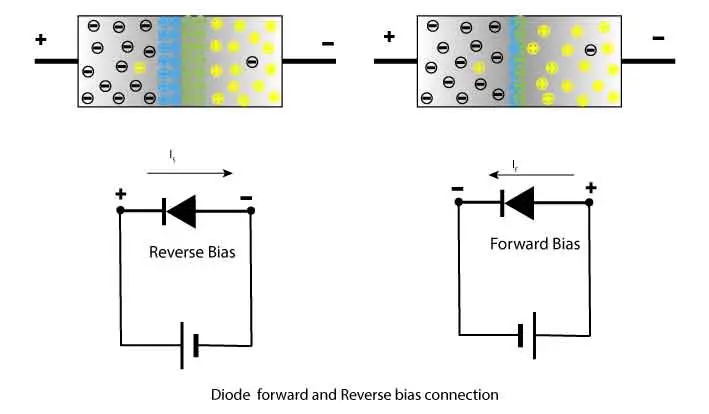
Operating Modes of a PN Junction Diode
The behavior of a diode depends on how the external voltage is applied.
Forward Bias
Forward bias occurs when:
- The positive terminal of the supply is connected to the P-side
- The negative terminal is connected to the N-side
This external voltage reduces the built-in potential barrier.
As the applied voltage increases:
- Depletion region narrows
- Barrier potential decreases
- Charge carriers cross the junction
Once the applied voltage exceeds the threshold (about 0.7 V for silicon):
Current flows rapidly.
In forward bias:
The diode behaves like a closed switch.
Applications:
- Rectifiers
- Signal clipping
- Voltage regulation
Reverse Bias
Reverse bias occurs when:
- The positive terminal is connected to the N-side
- The negative terminal is connected to the P-side
This external voltage increases the built-in potential barrier.
As a result:
- Depletion region widens
- Carrier movement is blocked
- Current becomes extremely small
Only a tiny current flows due to minority carriers. This is called reverse leakage current.
In reverse bias:
The diode behaves like an open switch.
However, if reverse voltage becomes too high:
Breakdown occurs (Zener or avalanche breakdown), and a large current can flow.
Applications:
- Rectification
- Clipping and clamping circuits
- Voltage regulation (Zener diode)
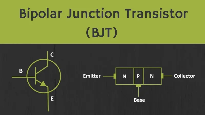
Transistors
Transistors are semiconductor devices used to amplify signals and act as electronic switches. They are the fundamental building blocks of modern electronic systems, including microprocessors, communication devices, and control systems.
There are two primary types of transistors used in electronics engineering:
- Bipolar Junction Transistor (BJT)
- Metal Oxide Semiconductor Field Effect Transistor (MOSFET)
Although both perform similar functions, they operate differently.
Two main types:
Bipolar Junction Transistor (BJT)
A BJT is a current-controlled device.
It consists of three regions:
- Emitter
- Base
- Collector
There are two types:
- NPN
- PNP
How It Works
In a BJT, a small current flowing into the base controls a much larger current flowing from collector to emitter.
Relationship:
Collector current ≈ Beta × Base current
Where Beta (β) is the current gain.
This means a tiny base current can control a much larger output current.
Why It Is Called “Bipolar”
It is called bipolar because both charge carriers participate:
- Electrons
- Holes
Applications of BJT
- Signal amplification
- Audio amplifiers
- Small-signal circuits
- Switching applications
In amplification mode, BJTs are widely used in analog electronics.
In switching mode, they behave like an ON/OFF device.
MOSFET
A MOSFET is a voltage-controlled device.
It also has three terminals:
- Gate
- Drain
- Source
Unlike a BJT, the MOSFET does not require input current at the control terminal. Instead, it uses an electric field.
How It Works
When voltage is applied to the gate, it creates an electric field that controls current flow between the drain and the source.
No significant current flows into the gate.
This makes MOSFETs:
- Highly efficient
- High input impedance devices
Why It Is Important
Because it requires almost no input current, the MOSFET:
- Consumes less power in control circuits
- Generates less heat
- Is ideal for digital systems
Applications of MOSFET
- Microprocessors
- Digital logic circuits
- Power converters
- Motor control systems
- Switching power supplies
Modern integrated circuits contain millions or billions of MOSFETs.
Analog Electronics
Analog electronics deals with continuously varying signals.
Key circuits include:
- Amplifiers
- Oscillators
- Filters
- Voltage regulators
Amplifiers increase signal strength without distortion.
Filters shape frequency content.
Oscillators generate periodic signals.
Analog systems are crucial in audio systems, sensors, and instrumentation.
Digital Electronics
Digital electronics operates using discrete binary levels (0 and 1).
Core elements:
- Logic gates
- Flip-flops
- Counters
- Multiplexers
- Microcontrollers
Digital circuits form the basis of:
- Computers
- Communication systems
- Embedded systems
- Industrial controllers
Binary logic enables reliable data processing.
Operational Amplifiers (Op-Amps)
Op-amps are versatile integrated circuits used for signal conditioning.
Common configurations:
- Inverting amplifier
- Non-inverting amplifier
- Voltage follower
- Integrator
- Differentiator
Op-amps are used in:
- Signal amplification
- Filtering
- Control systems
- Instrumentation
They simplify complex analog designs.
Power Electronics
Power electronics focuses on the control and conversion of electrical power using semiconductor devices.
Includes:
- Rectifiers
- Inverters
- DC-DC converters
- Switching regulators
Applications:
- Solar inverters
- Electric vehicles
- Motor drives
- Renewable energy systems
Power electronics bridges electronics and large-scale electrical systems.
Communication Electronics
Electronics plays a major role in communication systems.
Core topics include:
- Modulation techniques
- Signal transmission
- RF circuits
- Antennas
Modern wireless systems depend heavily on electronic circuit design and signal processing.
- Surge Protection in Plain English: When SPD’s Are a Must
- NSW Service & Installation Rules: What Changed in 2025
Embedded Systems
Embedded systems combine hardware and software to perform specific tasks.
They consist of:
- Microcontrollers
- Sensors
- Actuators
- Firmware
Applications include:
Embedded systems represent the future of electronics engineering.
Practical Applications of Electronics Engineering
Electronics engineering impacts:
- Consumer electronics
- Industrial automation
- Medical equipment
- Renewable energy systems
- Robotics
- Telecommunications
Nearly every modern device contains multiple electronic subsystems.
Skills Required in Electronics Engineering
To excel in electronics:
- Strong circuit analysis fundamentals
- Semiconductor device knowledge
- PCB design understanding
- Simulation skills (e.g., SPICE tools)
- Problem-solving ability
Continuous learning is essential given the rapid pace of technological evolution.
Common Challenges in Electronics Design
- Noise interference
- Thermal management
- Signal distortion
- Power losses
- Electromagnetic compatibility
Proper analysis and simulation reduce design failures.
FAQs
Electrical engineering deals with power systems, while electronics focuses on low-voltage signal processing and semiconductor devices.
It requires strong fundamentals, but with consistent practice and practical exposure, it becomes manageable and rewarding.
Yes. Solar inverters, battery management systems, and smart grids rely heavily on electronics.
Final Thoughts
Electronics engineering is the driving force behind modern technology. From semiconductor physics to advanced digital systems, it blends theory with innovation. Mastering electronics requires strong fundamentals, practical experimentation, and continuous exploration of emerging technologies.
This guide provides a structured overview to support your learning journey and connect foundational theory with real-world engineering applications.