What is a FET? FET is an electronic component that is used in many electronic circuits and appliances. FET is a three-terminal Three-layer device used for switching purposes like a BJT transistor. FET stands for Field Effect Transistor. Learn the FET Transistor basics in this article.
- Basic Electrician Test – Check Your Electrical Knowledge
- Complete Guide to Circuit Analysis in Electrical Engineering
What is the Difference Between Bipolar Transistors and Field-Effect Transistors (FET)?
- The main difference between the BJT transistor and the FET transistor is the controlling parameter. BJT is a current-controlled device, while FET is a voltage-controlled device.
- BJT is a bipolar device, whereas the FET is a unipolar device. Bipolar means that the current in the BJT flows due to electrons and holes. A unipolar transistor means that the FET is current due to either electrons or holes.
FET Transistor Basics
We are familiar with the concept that a static charge produces an electric field around itself. The electric field can pull other charges. The same phenomenon can happen inside the semiconductor. The electric field inside the semiconductor channel can attract charges and control the path of conduction inside the channel.
FET Transistor Construction
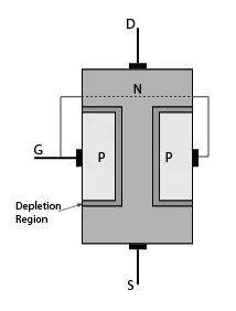
The construction of an n-channel JFET has three terminals and two junctions. The major portion of the structure consists of n-type material for the n-channel JFET. The two P-type materials are deposited on both sides of the n-channel, forming two PN junctions. Where the deposition is made, the n-channel area for conduction reduces. Both sides of the n-channel are connected to the electrodes. One terminal is the drain, and another terminal is the source. Where both P-type materials are connected to the gate terminal. The gate terminal is the controlling terminal of the source to drain the current.
How does a FET Transistor Work?
- Charging EV: A Beginner’s Guide to Electric Vehicle Ownership
- 3D Scanning in Industrial Inspection and Engineering Applications
Let’s discuss the FET working for different cases of gate and source-drain input. Consider the following cases.
- No Gate input
- Negative Voltage at Gate
No Gate Input VGS=0
For the n-channel JFET, suppose a positive drain-to-source voltage VDS is applied. And the input at the gate to source voltage VGS is zero volts. The PN junction between the gate and n-channel is reverse-bias and forms a depletion region around the junction. For the drain to source voltage VDS, the drain current ID will flow, limited only by the n-channel ohmic resistance.
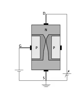
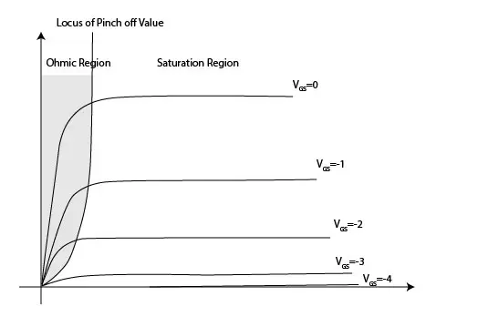
By increasing the drain to source voltage VDS from zero voltage, the drain current ID will increase. The current at this stage can be determined by Ohm’s law. Due to the increasing reverse voltage, the depletion region will become wider. At some point at a few voltages of VDS, the depletion region will become so wide that there will increase in current for an increase in voltage. That value of VDS is called pinch-off voltage VP. Further, an increase in VDS will not increase the current ID. This maximum current of ID is called IDSS.
Negative gate voltage input VGS<0
By applying the negative gate voltage input of the gate to the source voltage VGS, different curves are obtained. For different VGS, similar characteristics of JFET can be obtained, but have lower drain current. This means for more VGS, the pinch-off voltage will reach faster, and IDSS will be lower. The amount of VGS that results in zero drain current is called the pinch-off voltage, denoted by VGS(off). The region at the left of the pinch-off voltage locus is the linear region for amplification.
Voltage Controlled Variable Resistor
The region to the left of the pinch-off voltage and locus curve is called the ohmic region or voltage-controlled resistor. In this region, the JFET can work as a voltage-controlled variable resistor.
FET Transistor Symbols
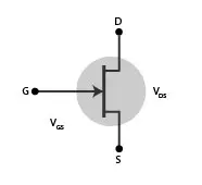
The FET symbol has three terminals: gate, drain, and source. The gate is highlighted by the arrowhead. Where the arrowhead points to the conventional current if the PN junction is forward-biased.
Types of FETs
FET can be categorized in different ways. All the types of FET are covered in the following FET tree diagram.
FETs are mainly categorized into junction and insulated gate type FETs.
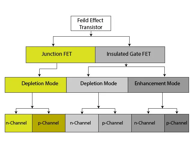
JFET Transistor
JFET transistor refers to the FET that has a junction between the gate and channel. The reverse bias of the junction controls the drain current. The JFET can be further divided into n-channel and p-channel devices.
Insulated Gate FET IGFET or Metal Oxide Silicon FET MOSFET
Insulated Gate FET is a broad category where Metal Oxide Silicon FET MOSFET is the most well-known insulated gate FET available in the market. MOSFET has metal oxide over the silicon substrate to construct an FET for insulation purposes. The most prominent feature of MOSFET is the high input impedance.
Dual-Gate MOSFET
Dual-Gate MOSFET uses two gates along the channel to improve the performance of RF signals. The second gate provides more insulation. The dual-gate MOSFET can be used for mixing and multiplication purposes.
Meta Silicon FET MESFET
Meta Silicon FET MESFET is fabricated using Gallium Arsenide and used for RF applications. It can provide high gain and low noise. MESFET has a very small gate structure; therefore, it’s very risky to handle the MESFET.
HEMT / PHEMT
HEMT / PHEMT High Electron Mobility Transistors or Paedomorphic High Electron Mobility Transistors are JFET modifications for higher frequency and high-performance applications.
- Crane Electrical Systems: Safe, Intelligent, and Efficient Operation
- Electrical Installation Guide: Wiring, Protection & Safety Standards
FINFET
FINFET is used inside the integrated circuit due to its smaller size. For the higher component density of IC FINFET is used more widely.
VMOS
VMOS stands for vertical Metal Oxide Silicon. VMOS can improve the current flow in the vertical direction. VMOS FET is used for power electronics applications.
Short Answer Questions:
When to use a BJT transistor, when to use an FET, and when to use a MOSFET?
Choose a Bipolar Junction Transistor (BJT) for analog and moderate-power switching, a Field-Effect Transistor (FET) for high-input impedance applications like RF circuits, and a MOSFET for digital and efficient power switching in applications like integrated circuits and power electronics.
Are Field Effect Transistors Fast?
Yes, field-effect transistors (FETs), particularly MOSFETs, are known for their high speed. They are commonly used in applications where rapid switching and fast response times are essential. They can operate across a broad frequency range.
What is a FET microphone?
A FET (Field-Effect Transistor) microphone is a type of condenser microphone that uses a FET as an impedance converter. It provides high sensitivity and low noise, and is commonly used in professional audio recording applications.
That’s a great article. I am glad that such a view is available for beginners.