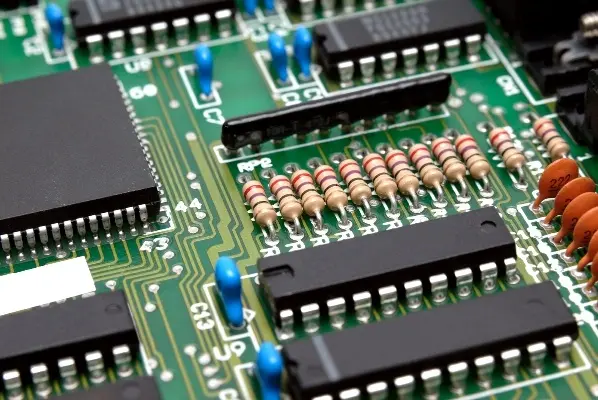
The printed circuit board is the heart of any electronic device, ranging from cell phones to vehicles. A layman can recognize it as a green board with lines over it and electrical components connected to it with solder. The green color is characteristic of the solder mask. Every PCB has a component connected to it. It is PCB assembly, and the process is the PCB assembly process. In an assembled PCB, components are connected by copper lines called traces to complete a specific circuit. The process of PCB assembly is simple and can be performed manually and/or automatically. Here is an example of a PCB assembly company that is located in the USA. PCB companies range in size and industry. There are also OEMs (original equipment manufacturers) that assemble their PCBAs, depending on the technology.
- Charging EV: A Beginner’s Guide to Electric Vehicle Ownership
- 3D Scanning in Industrial Inspection and Engineering Applications
Parts of the PCB
Layers
PCB consists of one to several layers, and every layer plays an important role in the completion of the circuit.
Substrate
A substrate is a rigid material that makes a PCB tough and provides housing for components.
Copper
A layer of copper is where all the circuit is completed. The copper layer allows the current to flow from one component to another using copper foils with specific lines known as traces. Based on the availability of copper foil, PCB may be regarded as a single-sided PCB or a double-sided PCB.
Solder Mask
Solder Mask avoids an unintentional short circuit above the copper layer. The mask gives the PCB a green color and is an insulating material.
Silk Screen
The silkscreen is used for labeling the PCB and symbolizing to identify the components and their function.
Types of PCB
There are three types of printed circuit boards.
Rigid PCB
These printed circuit boards are inflexible and rigid. These types of PCBs are commonly used. The substrate of the PCB is made from fiberglass, FR4, epoxies, or phenolics.
Flexible PCB
These are flexible circuit boards and it is bendable. The substrate is made with a high-temperature Kaplan.
Metal Core PCB
These are alternatives to rigid PCBs as the metal core dissipates heat easily and protects expensive components and devices.
- Basic Electrician Test – Check Your Electrical Knowledge
- Complete Guide to Circuit Analysis in Electrical Engineering
Technology
There are two mounting technologies in the printed circuit board assembly.
Thru-Holes Technology
Thru-hole technology is used for components with leads and wires. Components leads are plugged into the holes of the PCB and are soldered on the other side of the board with traces. This technology is used for large components like capacitors and inductors.
Surface Mount Technology
Small components like diodes and resistors are placed on the top of the board without any holes. Surface mount technology can place a Surface Mount Device (SMD) on the PCB.
PCB Assembly Process
Solder Paste Stenciling
A stencil of solder paste is applied to the PCB board. The process only allows the solder to the placed where the components are connected in the final PCB. Solder is a metal substance that contains tin 96%, silver 3%, and copper 1%. A machined fixture holds the stencil and PCB both in place, the applied solder paste is spread for even distribution, and then the stencil is removed, leaving the solder paste in specific locations. There are good companies that elevate your electronic designs with PCB Trace Manufacturing, where precision meets passion in every circuit board.
Pick and Place
After the removal of the solder stencil, components are placed and soldered on the board using robots. Traditionally,y the task was performed manually.
Reflow Soldering
The components are kept in place, and the PCB is moved across a reflow oven using a conveyor belt. The temperature of the oven is about 250 degrees Celsius. This high temperature melts the solder paste and connects the components to the board. After the oven, the PCB boards are passed through coolers. A double-sided PCB is passed through a reflow oven twice.
Inspection
The PCB is now inspected and tested. The reflow process can result in poor connections, missing components, or extra connections. The checking of the board may involve manual checking, automatic optical inspection, or X-ray inspection.
- Crane Electrical Systems: Safe, Intelligent, and Efficient Operation
- Electrical Installation Guide: Wiring, Protection & Safety Standards
Thru-Hole Insertion
Depending upon the requirements of the board, components should be inserted into the holes beside the SMDs. PTH components require a more specific type of process, like manual soldering or wave soldering. In the manual process, the components are inserted and soldered by a technical person in multiple cycles. In wave soldering, the PCB is passed through a conveyor belt.
Final Inspection and function testing
Finally, PCB boards a tested for their functionality by simulating normal circumstances where the PCB will operate later. An electrical signal runs through the PCB, and the electrical characteristics are observed. If a PCB board gives an unexpected response, the PCB is regarded as a failure based on company policy.
Cleansing
In the Turn-key PCB Assembly process, the PCB is cleaned for residual soldering paste and flux, which can damage the solder with time and affect customer satisfaction. High-pressure Deionized water is used for cleaning the PCB.
Short Answer Question:
What is the difference between PCB and PCB Assembly?
A PCB (Printed Circuit Board) is like the foundation for electronic components, and a PCBA (Printed Circuit Board Assembly) is the process of putting those components onto the board to make it work.