A Bipolar Junction Transistor (BJT) is a three-layer and three-terminal device having two PN junctions. The bipolar junction BJT transistor is made up of two N-type and P-type materials. In the case of NPN or two P-type and a single N-type material, making three two-junctions. Transistors are mainly used as switching devices or as amplifiers.
Construction of BJT Transistor
A Bipolar Junction Transistor is a three-layer device where every layer is connected by an electrical connection. The three terminals are called Emitter E, Base B, and Collector C. An NPN transistor can be formed by doping a sandwich of P-type material between two N-type materials. Similarly, a PNP transistor is formed by doping a sandwich of an N-type layer between two P-type layers. There are two PN junctions in a transistor. The first junction is a base-emitter BE junction, and the second one is called a base-collector BC junction.
- Basic Electrician Test – Check Your Electrical Knowledge
- Complete Guide to Circuit Analysis in Electrical Engineering
In either NPN or PNP, the emitter E is heavily doped, the base B is lightly doped, and the collector C is moderately doped. The outer layers are wider than the central layer. The ratio of the total size of a transistor to the base is 150:1. The doping of the central layer is also less compared to the outer layers by a 10:1 ratio. This increases the resistance of the layer by limiting the number of carriers. The transistor is called Bipolar because the transistor current is made up of hole and electron currents.
Symbol of BJT Transistor
The symbol of the transistor contains a three-terminal representation of the Emitter, Base, and Collector. The Emitter terminal is differentiated by an arrowhead from the Collector terminal. The direction of the arrowhead shows the type of transistor (NPN or PNP). The direction of the arrowhead shows the conventional current flow. In the case PNP transistor, the arrow points inside, and for an NPN, the arrow points outside the transistor.
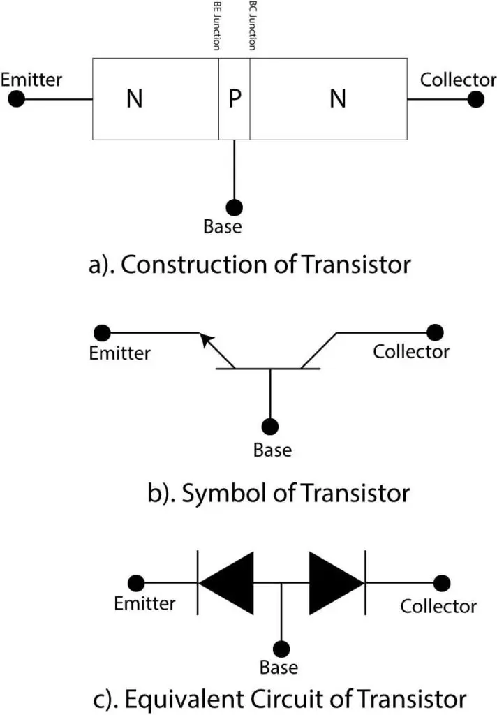
Equivalent circuit
The transistor equivalent circuit contains two back-to-back diodes. In the case of the NPN transistor, the anode terminals of both diodes are shorted and named as the base. In the case of the PNP transistor, the cathode terminal is shorted and named as the base terminal of the diode.
Working principles of the BJT transistor
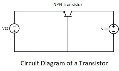
For a properly working transistor, it should be connected to DC voltages at all three terminals such that both of the PN junctions are correctly biased. The base-emitter junction should be forward-biased, and the base-collector junction should be reverse-biased. The working of NPN and PNP transistors is the same except for the role of electrons and holes, biasing voltage polarities, and direction of current flow.
- Charging EV: A Beginner’s Guide to Electric Vehicle Ownership
- 3D Scanning in Industrial Inspection and Engineering Applications
As the BE junction is forward-biased and the BC junction is reverse-biased, the BE depletion region becomes narrow, and the BC depletion region widens. The heavily doped emitter can easily inject electrons (in NPN) to baes and is called emitter current IE. As the base is lightly doped, only a few electrons recombine with holes at the lightly doped base and become base current IB. Where the rest of the electrons cross the BC junction due to the electric field developed by the positive and negative ions. It becomes the collector’s current IC.
FAQs
Can we use a BJT as a diode?
Though a bipolar transistor comprises two diodes, it’s not intended for direct use as a diode.
Why is a BJT called a current-controlled device?
As the base current changes, it influences the collector current proportionately, demonstrating the direct relationship between input and output currents in a BJT.
Is a BJT symmetric or asymmetric?
Bipolar junction transistors (BJT) are asymmetric; interchanging the collector and emitter terminals can cause the transistor to operate in reverse mode rather than the forward active mode.
Which is faster, BJT or MOSFET?
MOSFETs are typically faster than BJTs due to their majority carrier current conduction. The absence of minority carriers results in quicker switching times compared to BJTs.