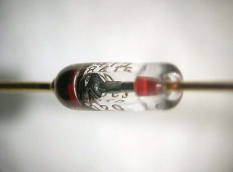
PN Junction diodes are made by doping the trivalent element into one side of an intrinsic semiconductor like silicon and doping the pentavalent to the other side. The side of the trivalent element will become P-type material, whereas the side of the pentavalent element will become N-type material. As far as both types of material are on the same substrate, a point of conjunction will exist there, which is called a PN Junction.
We have seen previously that the doping of trivalent and pentavalent ions into germanium or silicon can produce P-type and N-type materials. In N-type materials, the pentavalent atom makes four covalent bonds with the silicon atom, and one electron remains unbound, which can move freely and is called a free electron. There are more free electrons in N-type material than holes, which are caused by impurities in the intrinsic semiconductor. The electrons are referred to as majority carriers, and holes are referred to as minority carriers N-region of the PN Junction. Similarly, in P-type material, a trivalent atom makes three covalent bonds with a silicon atom, and one room remains left to bond with silicon, which is called the hole. There are more holes, which are called majority carriers, than thermally generated free electrons, which are called minority carriers. Remember that the number of electrons and protons in both N-type and P-type materials is the same, so they are electrically neutral.
- Charging EV: A Beginner’s Guide to Electric Vehicle Ownership
- 3D Scanning in Industrial Inspection and Engineering Applications
If one side of an intrinsic semiconductor substrate is doped with a trivalent and another with a pentavalent element, the whole substrate will be called a PN junction diode. A question may be raised that this new substrate would be unstable, all electrons and holes will combine, and the PN junction substrate will lose its meaning. Let us have a look at the internal situation inside the substrate.
Depletion region Formation:
At the instant of doping, free electrons near the junction from the N-type region pass the joining point toward the P-type region and combine with a hole near the junction. As the N-type region loses electrons and the P-type regions lose holes, they are not electrically neutral. But a small region near the junction in the P-type region becomes negatively charged, and similarly, a small region near the junction N-type region becomes positively charged. Both these charged regions are collectively called depletion regions, which contain neither free electrons nor holes. This depletion region is very thin and is formed very quickly.
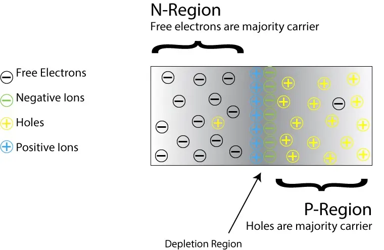
After the first surge, the very thin depletion region expands to some extent and makes it impossible for free electrons to pass the region and diffuse into the other side. As the electrons diffuse to the P-type region, the negative charge increases inside the P-type after some diffusion, and the negatively charged region in the P-type repels the diffusion of electrons. Thus, after the formation of the depletion layer, no free electrons can pass the depletion region.
Potential Barrier:
After the formation of the depletion layer, these positive and negative charges are held together across the junction. According to the Coulomb law, these charge regions across the junction will exert forces on each other. These charges will form an electric field that opposes the passage of free electrons from the N-region to the P-region. External energy is required for electrons to pass through the electric field. The potential difference required for electrons to pass through the electric field produced by the depletion region is called the Barrier Potential. After the application of this voltage in proper polarity, the electron from the N-region can get into the P-region. The amount of barrier potential depends upon the doping level, temperature, and semiconductor material. The typical barrier potential for silicon is 0.7V, and that for germanium is 0.3V at room temperature.