A diode is a terminal electronics component that can be connected to the source in two different ways: forward bias and reverse bias. The forward-biased diode acts like a closed switch, allowing current to flow through it. In contrast to the forward bias, the reverse bias diode blocks the current passage and works as an open switch. The biasing of a diode depends upon the direction of the source.
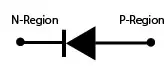
As we have discussed, the diode is made of a PN junction having one side of the P-type material and another of the N-type material. A depletion region is formed at the time of manufacturing, where electrons and holes combine to form ions, and no carrier is available for conduction in the region. The n-region has free electrons as majority carriers, and the P-region has a hole (absence of an electron). During the absence of an external voltage source, because of the random movement, minority carriers can enter the depletion region. Any hole entered into the depletion region will be attracted to the P-region, and the free electron will be attracted to the N-region by the attraction force of opposite ions in the depletion region. Some minority carriers may enter the P-type, and others may enter the N-type, and ultimately, there will be no net current flow.
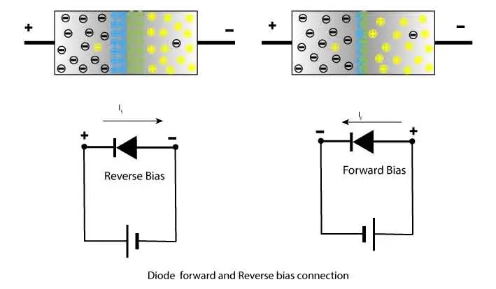
Reverse Bias Diode:
In Reverse Bias, the anode terminal of the voltage source is connected to the N-type pin, and the cathode terminal of the voltage source is connected to the P-type pin of the diode. In the reverse bias diode operation, the diode acts like an open switch. The anode terminal of the source will draw the free electrons from the N-type, and the cathode will draw the holes from the P-type. Thus, the number of ions in the N-region and P-region will increase, which is the reason for the widening of the depletion region.
- Charging EV: A Beginner’s Guide to Electric Vehicle Ownership
- 3D Scanning in Industrial Inspection and Engineering Applications
However, the minority carrier will enter the depletion region and pass to the other side of the junction, causing a small current. This small amount of current is called the reverse saturation current and is represented by Is. The term “saturation” shows the fact that after a very short change of the current for a change in voltage, the current will not increase anymore with increasing the reverse bias voltage.
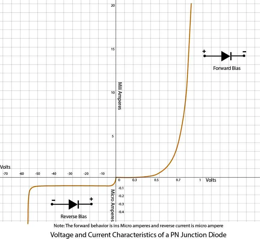
In the V-I characteristic curves, the graph in the third quadrant represents the reverse behavior of the diode. In the beginning, the current changes very quickly for a small change in voltage and reaches the saturation current. The further changes in the voltage do not affect the current.
For tens of volts in reverse bias, the current remains constant. But reaching a high reverse voltage causes a huge current in the reverse direction. As the reverse voltage increases, the velocity of the reverse current increases as well as its kinetic energy. The high kinetic energy is transferred to the valence shell electrons of stable atoms and makes them leave the atom. These additional carriers can aid in the reverse current flow. The voltage at which this rapid change in current occurs is called Zener Voltage and is represented by VZ. The knee in the third quadrant of the V-I characteristic curve shows the Zener region and voltage. Special diodes like Zener diodes and photodiodes are operated in reverse bias.
Forward Bias Diode :
A diode is forward biased if the P-type pin is connected with the anode of a voltage source and the N-type of the diode is connected with the cathode of the source. In forward-bias diode operation, the diode acts like a closed switch. The voltage source in the forward bias configuration applies pressure on free electrons in the N-region and holes in the P-region toward the depletion region. The free electrons and holes recombine with the ions near the depletion region, and the depletion region width is reduced. Then the majority carrier can pass the thin depletion region. As the forward bias voltage increases, the depletion region width decreases, and more and more carriers can pass.
The first quadrant of the V-I characteristics curves shows the forward operation of the diode. In the beginning, by increasing the voltage, the current changes very slowly, but when the voltage reaches 0.7V (for silicon), the current starts to change rapidly for a small change. The rapid change in the current shows that the resistance decreases as we increase the voltage above the knee of the curve. The voltage drop across the diode in the forward bias is equal to the barrier potential, but may increase up to 0.9, depending upon the current.
Diode Biasing Keypoints:
- For no external voltage, there is no net current flowing in the diode.
- A forward-bias diode means connecting the anode to the P-type and the cathode to the N-type.
- The diode acts as a closed switch in the forward bias.
- A reverse bias diode means connecting the anode to the N-type and the cathode to the P-type.
- The diode acts as an open switch in Reverse bias.
The polarity on the upper pictures (the squares with + and – inside) seems wrong. It is not aligned with the equivalent circuit below.
Thanks for your suggestion. It is corrected.
Can you do this in excel? i would like to know the behavior of the real diode formula on excel applied on this
Hopefully, you are talking about VI Characteristics curves.
These curves are for real diodes. Anyone with a diode, variable voltage supply, and multimeter can verify the curves.
Where the formula for diode current is here at the link: https://electric-shocks.com/diode-equation/
Its excel formula is: (for Germanium )
=A1*EXP(40*B1-1)
if A1=Io and B1= V