All industrial and domestic electronic devices are made of a semiconductor. As the name suggests, semiconductor materials are neither good conductors nor good insulators of electrical currents, like Silicon and Germanium. Because of the very few current carriers (free electrons) available in the conducting shell. The specific resistance of the materials is comparatively higher than that of a conductor and lower than that of an insulator. The difference between intrinsic and extrinsic semiconductors is the number of carriers. The number of carriers is higher in extrinsic semiconductors, i.e., P-type and N-type semiconductors.
Semiconductors are the perfect insulator at 0oK temperature. At a higher temperature, the materials are neither conductors nor insulators. The energy gap of semiconductors is lower by almost 1ev. At normal temperatures, when electrons in the valence shell gain energy, the gap between the valence band and conduction band is reduced. Very few electrons become available at the conduction band, so a very low current flow could be expected.
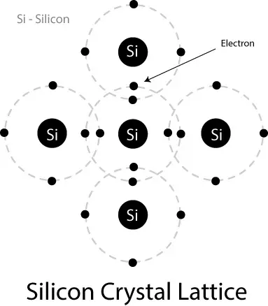
Germanium and Silicon are the most widely used semiconductors, and both belong to the 4th column of the periodic table, which means they have 4 electrons in their valence shell. They have a single-crystal structure; each atom in a structure is connected to four other atoms by a covalent bond, which means there will be no free electrons in a crystal. But electrons can absorb external energy, like light/heat, to escape the bond and freely move.
Difference between intrinsic and extrinsic semiconductors:
The essential difference between intrinsic and extrinsic semiconductors is the number of carriers. The number of carriers is improved by doping impurities. An intrinsic semiconductor has a low carrier concentration.
Intrinsic Semiconductor:
Germanium and Silicon may have some impurities that can cause them to lose their property and conduct more current than expected. These semiconductors can be purified by the use of modern technology, which is called Intrinsic Semiconductors. The intrinsic semiconductor has very few free current carriers at room temperature. As the temperature increases, electrons gain energy and become free electrons, and ultimately resistance of the material decreases, which is a negative temperature coefficient.
Extrinsic Semiconductor:
The electrical characteristics of an intrinsic semiconductor are not that beneficial. The characteristics can be changed by introducing some impurities in the intrinsic semiconductor, like pentavalent and trivalent elements, then that material is called an extrinsic semiconductor material. The operation of introducing impurities is called the doping process.
- Charging EV: A Beginner’s Guide to Electric Vehicle Ownership
- 3D Scanning in Industrial Inspection and Engineering Applications
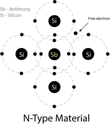
N-Type Semiconductor:
By doping a pentavalent element (Antimony), which has 5 electrons in the valence shell, four electrons of the shell make a covalent bond with four Silicon/Germanium atoms. The one-electron remains unbound, which is loosely connected to its parent atom and can move freely. The pentavalent element is called a donor. A new type of material is achieved through the process and is called N-type material.
It’s worth noting that the number of electrons and protons remains the same in the N-type material, so it remains electrically neutral.
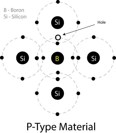
P-Type Semiconductor:
Similarly, in the impurities of the trivalent element (Boron, 3 electrons in the valence shell), all the electrons combine with surrounding Silicon/Germanium atoms, and a vacancy for a covalent bond remains. There is a place for one covalent bond, which is called a Hole. The trivalent element is called the acceptor because it has a place for an electron. So, the new material from the process is called P-type material.
Electron vs Hole current flow:
We are familiar with electron flow, but hole flow is something different. A hole is a vacant position where a covalent bond could be formed. If an electron from a covalent bond gets energy and escapes the bond, the electron can fill the hole and form a new band here. Thus electron will move in one direction, and the hole will move in the opposite direction.
Majority Carrier vs Minority Carrier:
In an intrinsic semiconductor material, there are always some free electrons and some holes available under normal conditions. Through the doping process of pentavalent impurity, the number of electrons can be increased. Similarly, by using a trivalent impurity, the number of holes can be increased. So, the N-type material has very few holes, and the P-type has very few free electrons. These few holes and free electrons are called minority carriers. While free electrons in N-type and holes in P-type are called majority carriers.
- Basic Electrician Test – Check Your Electrical Knowledge
- Complete Guide to Circuit Analysis in Electrical Engineering
Uses of Semiconductor
The uses of intrinsic and extrinsic semiconductors are different. But overall, semiconductor devices are used for all electronic devices nowadays, like diodes, transistors, and thyristors. Every electrical appliance has these semiconductor devices in it, whether it is a Television, Computer, or Refrigerator for home or industrial machinery like CNC machines, Telecommunication equipment, etc.
Thanks a lot for breaking it down and making it easier to understand