PCB boards are commonly used in every consumer electronics appliance. You may be familiar with PCB’s technical perspective, but may be missing some fun facts about PCB boards. Let’s dive in.
1. PCB has no Wires
Talking about the PCB board, it doesn’t have any wires on it. Even though it reduces the tedious wiring. The board passes current through the lower copper layer, which is called traces. For higher currents, the trace size is wide, and vice versa. The trace size is adjusted according to the requirement at the time of design.
- Crane Electrical Systems: Safe, Intelligent, and Efficient Operation
- Electrical Installation Guide: Wiring, Protection & Safety Standards
2. Why PCBs are Green
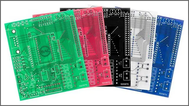
PBC board is not always green; it has many other variations, but green is more common among all the colors. The green color of the PCB is a solder mask. The solder mask helps against the oxidation of copper traces. It also prevents bridging in closely spaced soldering points. The color of the solder mask doesn’t matter at all, but the green color is the most common, and the rare ones are blue, red, black even white. However, the purpose is high contrast for identifying the components on the board.

3. What is the etching over the PCB?
Important information about the components is etched on the top of the PCB board. It’s called silkscreen. The silkscreen uses various electronics engineering symbols and terminology for identifying the component. It’s printed with a silkscreen or laser jet printer.
4. PCB is designed inside the Computer
PCB boards are designed in computer software called CAD software. The designer first draws a schematic diagram of the desired circuit as per the requirements of the clients. Then they can design the PCB layout out of the schematic diagram for testing. After the successful testing, the PCB design is passed on to the manufacturing plant for fabrication.
5. Every PCB has gold on it
Yes, you have heard it right. Every PCB board has gold on it. Because of the superior conductivity properties of gold as compared to silver and copper. On average, PCB has 140 to 700 grams of gold per tonne of PCB. You can extract that gold and utilize it. Here is a detailed article on how to extract gold from electronics without chemicals.
- Wearable Electronics: The Future of Smart and Connected Living
- Home EV Charger Installation Guide: Everything You Need to Know
6. PCB is getting smaller
As the electronic devices are reducing in size, it applies pressure on the PCB board to reduce in size. The evaluation of PCB size can be better understood by looking at the desktop, laptop, and handheld device sizes.
7. There are Wearable PCB Boards
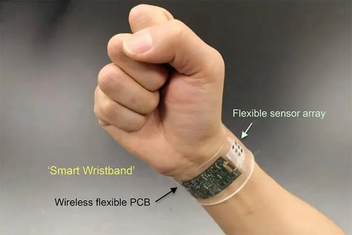
PCB boards are classically rigid, but there are flexible PCBs, even wearable PCB boards. Smartwatches, fitness trackers, Augmented reality headsets, Body-mounted sensors, smart clothes, smart jewelry, and AI hearing aids are some of the applications of wearable PCB boards.

8. PCB Trace Antenna
PCB Trace antenna is the last of the fun facts about PCB board. The antenna can be fabricated into the PCB board for wireless communication purposes. The antenna can transmit data over a certain distance wirelessly. It can reduce the cost as compared to the other type of antenna. The antenna is designed at the time of fabrication and may consist of single or multiple layers. But PCB trace antenna can be challenging for lower frequencies.