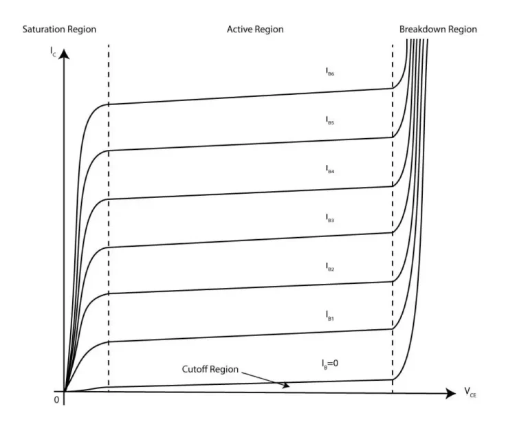
The collector characteristic curve shows the behavior of the transistor. To get these curves, we bias a BJT transistor with a variable power supply and change the VBB and VCC. By varying these voltages, either transistor PN junctions may be forward-biased or reverse-biased. Based on the condition of the BJT transistor junction biasing, the transistor can operate in four regions of operation.
Transistor Regions of Operation
Suppose we have an NPN transistor connected with variable power supplies, as the diagram shows.

Cutoff region
When the base power supply VBB is set to zero, the current IB becomes zero. Both of the PN junctions of the BJT transistor become reverse-bias, and no collector current IC flows. In this region, the transistor behaves as an open switch. The VCC voltage appears across the collector-emitter terminals VCE. This region is the cutoff region. This state is ideal for applications needing a switch that completely disconnects the circuit.
- Charging EV: A Beginner’s Guide to Electric Vehicle Ownership
- 3D Scanning in Industrial Inspection and Engineering Applications
Saturation region
When the collector supply VCC is set to zero, and the base supply is set to produce a certain base current IB. Both of the PN junctions become forward-biased. The base current IB flows through the emitter terminal because of low impedance, and no current flows through the collector IC=0. This Transistor region of operation is the saturation region. In this region, both junctions are forward-bias. The collector current IC reaches a certain maximum current independent of the base current IB. In the saturation region, the voltage across the collector-emitter terminals, VCE, is zero. This turns the BJT into a closed switch, making it indispensable in digital circuits where toggling between open and closed positions is critical.
The active or Linear region
By increasing the VCC, the voltage across the collector-emitter terminals VCE may increase. As the VCE passes the 0.7V, the base-collector PN junction becomes reverse-biased. And the emitter base is forward-bias. This mode of operation is the active or linear region of operation in the BJT transistor characteristic curve. By increasing the VCE beyond 0.7V, the collector current remains constant for a given value of base current IB. Increasing the VCE can cause a very slight increase in IC because of the widening of the base-collector depletion region. The following formula can calculate the active region collector current IC.
This configuration enables the transistor to amplify signals, making it vital for audio equipment, radio transmitters, and other applications where signal boosting is required.
Breakdown region
By increasing the VCC, the VCE can be increased, which may increase the reverse bias of the base-collector junction. The high reverse bias may cause widening of the base-collector junction and finally break down the junction. As the BJT transistor enters the breakdown region, the collector current will increase rapidly, as the diagram shows. A transistor is not used in the breakdown region.
- Basic Electrician Test – Check Your Electrical Knowledge
- Crane Electrical Systems: Safe, Intelligent, and Efficient Operation
Understanding Basic BJT Parameters
When discussing Bipolar Junction Transistors (BJTs), two fundamental parameters come into play: DC Beta (βDC) and DC Alpha (αDC).
DC Beta (βDC)
- Definition: DC Beta, often denoted as βDC, represents the DC gain of a transistor. It is calculated as the ratio between the DC collector current and the DC base current.
- Significance: βDC is crucial because it helps determine the transistor’s amplification capability—essentially, how much current the transistor can control.
- Variability: It’s important to note that βDC is not a fixed value. It varies with the collector current and the junction temperature. Typically, as the collector current increases, βDC rises to a peak before declining if the current continues to rise. Meanwhile, with a constant collector current, an increase in junction temperature will cause βDC to increase.
DC Alpha (αDC)
- Definition: DC Alpha, represented as αDC, is the ratio of the DC collector current to the DC emitter current.
- Usage: While αDCis less commonly used in practical applications compared to βDC, it remains an important parameter for understanding the efficiency of a BJT.
- Characteristics: The value of αDC is always less than 1 since the collector current is slightly less than the emitter current due to recombination losses in the base.
Conclusion
- Based on transistor characteristic curves, there are four regions of operation.
- The cutoff region works as an open switch
- The saturation region works as a closed switch
- IC remains constant for a certain amount of the IB active region
- The Breakdown region of a transistor is not used
FAQs
Why is a BJT called bipolar?
A BJT is named “bipolar” due to its operation relying on two charge carriers: holes and electrons.
What are the advantages of BJT?
Advantages of BJTs include superior performance in high-load and high-frequency conditions compared to MOSFETs. They offer higher fidelity, better gain in linear areas, and faster operation due to lower control pin capacitance than MOSFETs.
Thanks