
In the realm of Electrical and Electronics Engineering, the trajectory of innovation is driven by cutting-edge technologies and sophisticated tools that propel advancements. Among these tools, the prominence of EDA (Electronic Design Automation) tools stands out. These tools are the backbone of modern design, playing a pivotal role in optimizing circuits, systems, and processes. Let’s delve deeper into the world of EDA tools and uncover their significance in this domain.
Understanding EDA Tools
Electronic Design Automation (EDA) tools refer to software applications utilized in the design of electronic systems, including integrated circuits (ICs) and printed circuit boards (PCBs). These tools facilitate engineers and designers in developing, analyzing, and simulating electronic systems efficiently.
- Electrical Safety Test: 10 Quiz MCQs to Check Your Knowledge
- MCQs on Transistor BJT (Bipolar Junction Transistor)
The Versatility of EDA Tools
EDA tool offers a myriad of functionalities that cater to various aspects of Electrical and Electronics Engineering:
Circuit Design and Simulation:
EDA tools enable engineers to design and simulate electronic circuits, allowing them to assess performance, functionality, and potential issues before actual implementation. Programs like SPICE (Simulation Program with Integrated Circuit Emphasis) aid in simulating complex circuit behaviors accurately.
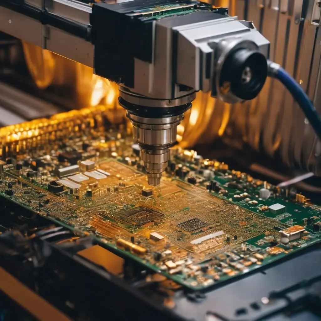
PCB Layout and Design:
These tools assist in creating PCB layouts, defining component placements, routing traces, and ensuring electrical connectivity. Software like Altium Designer and EagleCAD streamlines the PCB design process, enhancing accuracy and efficiency.
VLSI (Very Large Scale Integration) Design:
For complex integrated circuit designs, EDA tools like Cadence and Synopsys offer comprehensive solutions. These tools support the design and verification of intricate ICs, ensuring adherence to performance and manufacturing specifications.
Signal Integrity and Analysis:
EDA tools facilitate the analysis of signal integrity, ensuring that electrical signals propagate correctly and without distortion. This is crucial in high-speed designs to prevent issues like crosstalk and signal degradation.
The Impact of EDA Tools in Electrical and Electronics Engineering
The utilization of the EDA tool brings about significant benefits:
Enhanced Efficiency:
These tools streamline design processes, reducing manual effort and time required for development, thereby accelerating product innovation and time-to-market.
Improved Accuracy:
EDA tools enable detailed analysis and simulations, minimizing errors and allowing engineers to refine designs iteratively, leading to superior end products.
Cost Optimization:
By identifying issues early in the design phase, the tools help mitigate potential risks and prevent costly modifications during later stages of product development.
- Charging EV: A Beginner’s Guide to Electric Vehicle Ownership
- 3D Scanning in Industrial Inspection and Engineering Applications
Innovation Catalyst:
The tools empower engineers to explore novel design possibilities, pushing the boundaries of what’s achievable in Electrical and Electronics Engineering.
Conclusion
In the dynamic landscape of Electrical and Electronics Engineering, the tools emerge as indispensable assets, fostering innovation, optimizing performance, and revolutionizing design processes. Their multifaceted functionalities and profound impact make them indispensable for engineers and designers seeking to push the boundaries of technological possibilities.
As the forefront of innovation continues to evolve, leveraging the prowess of the tool remains fundamental for driving groundbreaking advancements in Electrical and Electronics Engineering.