An FPGA (Field-Programmable Gate Array) is a semiconductor device that can be programmed to implement a user’s desired logic circuits. Invented in 1985 by Ross Freeman, one of the founders of Xilinx, it is a type of Programmable Logic Device (PLD). The core advantage of FPGAs is their flexibility and reconfigurability, which allows them to be programmed in software to realize different functions without requiring hardware replacement. Research has shown that FPGA programming significantly differs from traditional software programming, as it involves hardware design rather than instruction sequences, and is particularly well-suited to high-performance computing, real-time processing, and custom logic needs.
The internal structure of an FPGA chip consists of a programmable logic block (CLB), an input/output unit (IOB), an embedded memory (BRAM), and a digital signal processing unit (DSP). The programmable logic block realizes various logic functions through look-up tables (LUTs) and flip-flops. This structure makes FPGAs widely used in communication, industrial control, medical equipment, aerospace, and other fields.
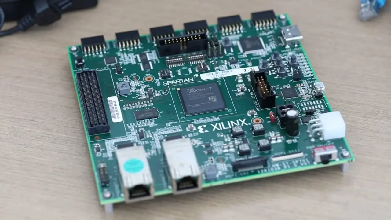
Xilinx is the leading vendor in the FPGA field, with a market share of about 50%, and its product lines include the Spartan, Artix, Kintex, and Virtex series, covering a wide range of needs from low-cost to high-performance. Xilinx FPGAs, known for their powerful development tools and rich IP libraries, are playing a key role, especially in the rapid development of 5G, AI, and the Internet of Things (IoT). Xilinx FPGAs are known for their powerful development tools and rich IP library, especially in the rapid development of 5G, AI, and IoT.
The Nature of FPGA Programming
FPGA programming is essentially configuring the logic units inside the FPGA to fulfill specific functions. While traditional software programming runs code on fixed hardware (e.g., a CPU), FPGA programming involves redesigning the hardware itself. Research has shown that this type of programming primarily uses hardware description languages (HDL) such as Verilog and VHDL, which allow engineers to describe the structure and behavior of digital circuits.
- 3D Scanning in Industrial Inspection and Engineering Applications
- Wearable Electronics: The Future of Smart and Connected Living
The programmability of FPGAs is referred to as hardware programmability, which is reflected in the fact that their internal circuit structure can be programmed to change to meet the application requirements of different hardware products. For example, in industrial automation, FPGAs are used to implement complex digital circuits and algorithms to improve device performance and reduce power consumption. Compared to ASICs (Application Specific Integrated Circuits), FPGAs offer higher flexibility and are suitable for low-volume production and rapid prototyping.
- Basic Electrician Test – Check Your Electrical Knowledge
- Complete Guide to Circuit Analysis in Electrical Engineering
Xilinx FPGA Overview
Xilinx is a leader in the FPGA industry with a portfolio of products that includes:
Spartan: low-cost, low-power for education and small projects.
Artix: Mid-range products for industrial control and communications.
Kintex: high-performance, mid-market for data centers and communications infrastructure.
Virtex: High-end product for ultra-high performance needs such as aerospace and scientific computing.
Zynq: SoC FPGAs with integrated ARM processors, combining the flexibility of a processor with the reconfigurability of an FPGA.
Xilinx FPGA features include the Vivado Design Suite, a powerful development tool that supports the full design-to-verification process; a rich IP library that simplifies the development process; and a wide range of application scenarios, from consumer electronics to the defense industry. Evidence shows that Xilinx FPGAs dominate the global FPGA market with a 52% market share in 2019, with strong demand especially in the Asia Pacific.
FPGA Programming Tools: Vivado Design Suite
Vivado is an integrated development environment (IDE) provided by Xilinx for designing, simulating, and verifying FPGA projects. It is the core tool for FPGA programming, and its key features include:
Project Creation: Define parameters such as FPGA chip type, clock frequency, and so on.
RTL Design: Write hardware description language code using Verilog or VHDL.
IP Integration: Add IP cores provided by Xilinx or custom IP.
Synthesis and Implementation: Convert HDL code into netlists that can be implemented on FPGAs and layout routed.
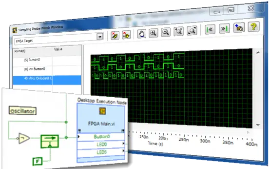
Simulation and Verification: Verify that the design is correct using Vivado’s simulator.
Bitstream File Generation: Finalize the bitstream file for download to the FPGA.

Additionally, for Zynq SoC FPGAs, Xilinx offers an SDK (Software Development Kit) for software development, which supports C/C++ programming, as well as the PetaLinux tool, which provides Zynq with Linux operating system development support. These tool chains make Xilinx FPGA programming more efficient and flexible.
Xilinx FPGA Programming Steps
The following is a summary of typical programming steps for Xilinx FPGAs, based on actual tutorials:
| Step | Description | Tools/Version | Remarks |
| 1. Install Vivado | Download and install the latest version of Vivado Design Suite (such as Vivado 2023.1). | Xilinx Vivado 2023.1 | Ensure the system is Windows or Linux. |
| 2. Create Vivado Project | 5. Build Block-level Design | – | – |
| 3. Import RTL Design | Import Verilog or VHDL files into the project to describe the digital circuit structure and behavior. | – | Example: calculator module, DATA_BW = 16. |
| 4. Create IP Package (Optional) | Package the RTL design as an IP core for easy reuse, using “Create and Package New IP”. | – | Refer to the tutorial pictures. |
| Use Block Design to connect different IP cores and add a Zynq Processing System. | Use Block Design to connect different IP cores and add Zynq Processing System. | – | Automatically connect AXI interfaces, etc. |
| 6. Verify Design | Use Vivado verification tools to check whether the design is correct and ensure that all connections meet the requirements. | – | Emphasize error checking. |
| 7. Synthesis and Implementation | Run Synthesis to generate a netlist, and run Implementation for placement and routing. | – | – |
| 8. Generate Bitstream File | Use the Generate Bitstream function to generate a file that can be downloaded to the FPGA. | – | – |
| 9. Download and Debug | Use JTAG or other interfaces to download the bitstream file and verify whether the design works properly. | – | Use Vivado debugging tools. |
These steps ensure that the design will run correctly on the FPGA and are suitable for beginners and professional engineers. Example address offsets: 0x43C00000 for ZedBoard and 0xA0000000 for ZCU102.
FPGA Chip Applications
FPGA chips have been widely used in the following fields due to their reconfigurability and high performance:
Communication: 5G base station, fiber optic communication, network switch.
Industrial control: machine vision, automation system, PLC.
Medical equipment: imaging equipment, ECG monitors.
Aerospace: satellite control system, flight controller.
Artificial Intelligence: machine learning gas pedal, neural network processing.
Automotive electronics: ADAS (Advanced Driver Assistance System), in-vehicle infotainment system.
Especially with the rapid development of 5G and AI, the market demand for FPGA chips continues to grow. According to market research, China’s FPGA chip market will reach 15.03 billion yuan in 2020, and is expected to further increase to 33.22 billion yuan by 2025, with a CAGR of 17.1%, higher than that of the global market of 10.85%. Asia-Pacific is the largest market, accounting for 39.15% of the total, and is expected to increase to 43.94% by 2025.
Advantages and Challenges of FPGA Programming
Advantages:
Flexibility: Designs can be modified on demand at any time, suitable for stages where the technology is not yet mature.
Performance: performs specific tasks more efficiently than general-purpose processors, especially in real-time processing scenarios.
Cost: more economical than ASICs in small volume production, reducing product development risk.
challenges:
Learning curve: FPGA programming requires knowledge of HDL and digital circuits, which may be difficult for beginners.
The development cycle, from design to verification, takes a long time, and resource optimization requires experience.
Resource constraints: FPGAs have limited logic resources and require trade-offs in the design.
Despite the challenges, the strong toolchain and documentation support for Xilinx FPGAs make it a worthwhile investment in skills. In particular, Vivado’s automation capabilities and rich community resources help engineers overcome learning barriers.
Conclusion
FPGA programming is an important skill in digital circuit design, and programming for Xilinx FPGAs in particular has become an industry standard. By mastering Vivado and HDL, you can realize the full potential of FPGAs for high-performance custom logic designs. With the rapid development of Artificial Intelligence, 5G, and the Internet of Things, FPGA applications are promising, and learning FPGA programming will open up endless possibilities for your career.